

(Gold finger or edge connector) will be inserted into the connector slot at one end of the pcb, using the connector pins of the connector as an external outlet of the pcb, so that the pad or copper skin and the corresponding location of the connector pins contact, to achieve the purpose of conduction, in the pcb of this pad or copper skin plated with gold or nickel gold, because of its finger shape and called gold finger.
Second, the gold finger PCB surface treatment
Electroplated nickel gold: thickness up to 3-50u". Because of its superior electrical conductivity, oxidation resistance and wear resistance, widely used in the need for frequent plugging and unplugging or frequent mechanical friction on the gold finger PCB. However, because of the high cost of gold plating, only used for gold fingers and other local gold plating. Jedobang PCB called "selective gold plating process". Gold plating process color is silver-white, unlike gold plating so yellow, the disadvantage is slightly worse solderability.
Three. Gold finger design considerations
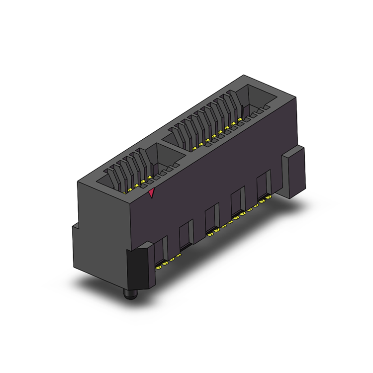
In the PCB design to see such a shape and package in the figure below, the first reaction is the board with gold fingers. A simple way to determine the gold finger: devices with pins on the upper and lower surfaces of the device; will be like the anti-dull U-slot in the figure below.
When there are gold fingers on the board, you have to deal with the details of the gold fingers.
PCB gold finger details processing:
1) For PCB boards that often need to be plugged and unplugged, in order to increase the wear resistance of gold fingers, gold fingers usually need to be hard gold plated.
2) gold fingers need to chamfer, generally 45 °, other angles such as 20 °, 30 °, etc.. If the design is not chamfered, there is a problem; as shown in the figure below, the arrow shows 45° chamfer:
3) gold fingers need the entire solder resist window openings to handle, the pins do not need to open the stencil.
4) Tin deposition and silver deposition pads need a minimum distance of 14 mils; from the top of the finger; improved design
when the pad is greater than 1mm from the finger position, including over-hole pads.
5) Do not lay copper on the surface of the gold finger.
The following figure is a gold finger design for reference:
6) gold finger inner layer of each layer need to cut copper, cut copper width is generally 3mm; can do half finger cut copper and whole finger cut copper. pcie design, gold finger area of copper are cut off.
The impedance of the gold finger will be relatively low. Cut copper (finger under the hollow) can reduce the impedance of the gold finger and impedance line impedance difference, but also conducive to ESD.
Suggestion: the copper below the gold finger pad are cut.
Fourth, Jie DuoBang PCB gold finger processing notes
1. Board thickness of 1.2-2.4m can be chamfered. In this thickness range can not be chamfered.
2. The depth and angle of the beveled edge is generally between 20-45 degrees by default. There should be enough distance between the gold finger and the board edge. According to the different gold finger PCB board thickness or design requirements, we recommend the design of the gold finger and the board edge distance of 0.6-1.5mm, so as not to hurt the gold finger in the beveled edge. If the distance between the gold finger and the board edge is less than 0.6mm, there will be a risk of hurting the gold finger if the beveled edge is needed to handle. Here are some common beveling angles and depth schematics for your reference.
Board thickness of 1.6mm, beveled edge depth of 1.4mm, bevel angle of 25 degrees.
Board thickness 1.6 mm, beveled edge depth 1.3 mm, beveled edge angle 25 degrees.
Board thickness 1.8 mm, beveled edge depth 1.8 mm, bevel angle 20-25 degrees.
Board thickness 1.2 mm, beveled edge depth 0.4 mm, bevel angle 45 degrees.